Exemplary Tips About What Is RTL To GDS

Lecture 1 Hand Written Notes VLSI Design FlowRTL To GDS NPTEL
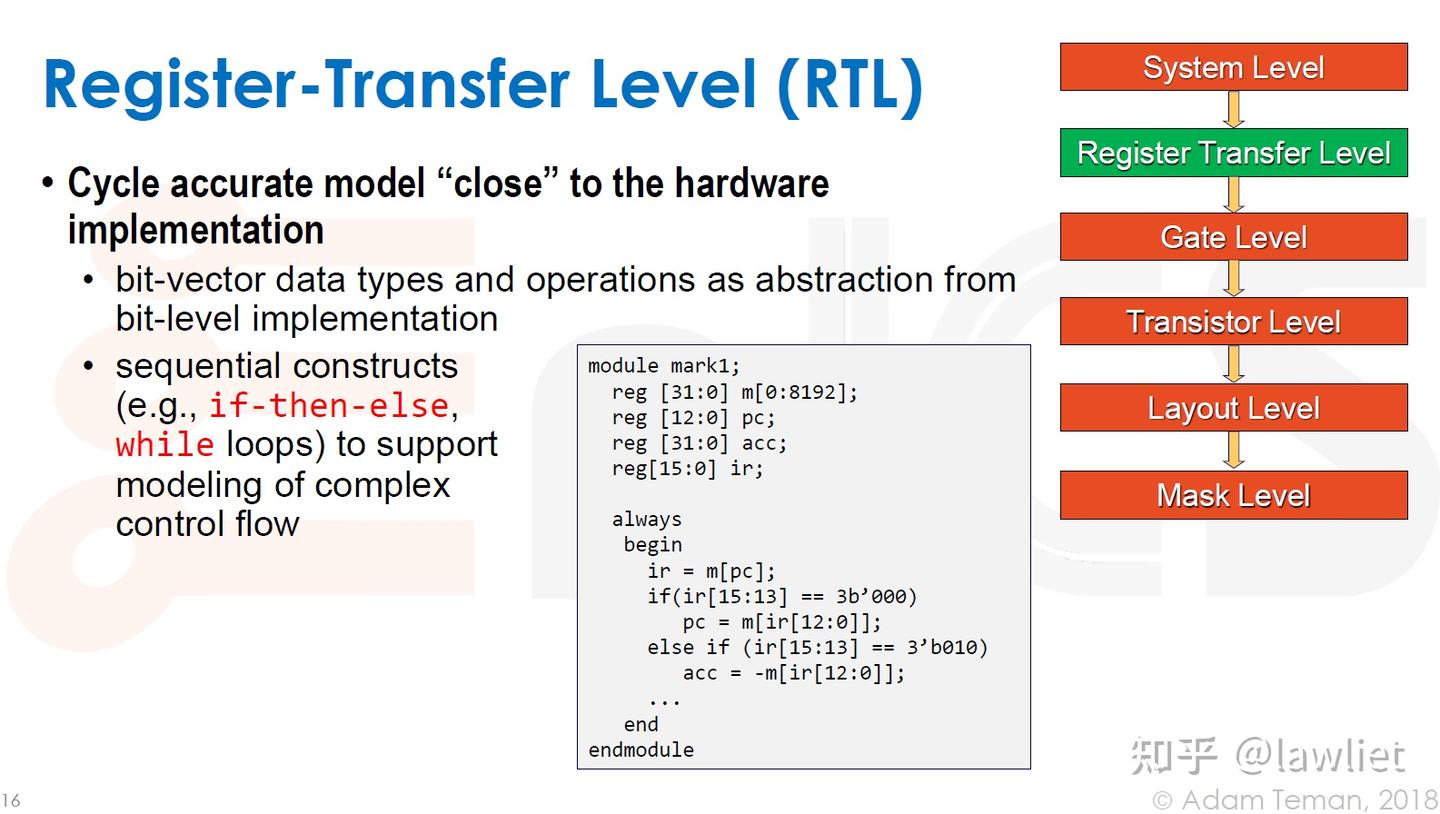
Decoding RTL to GDS
1. What's the Big Deal with RTL to GDS?
Ever wondered how a complex computer chip goes from a designer's idea to a physical reality? It's not magic, but it's pretty darn close! One key step in that journey is the process called RTL to GDS. Think of it as translating architectural blueprints (RTL) into instructions for building a house (GDS). Without it, we'd still be stuck with vacuum tubes the size of watermelons! So, yeah, it's kind of a big deal. This article dives into exactly what RTL to GDS is, why it matters, and how it all works.
Register Transfer Level (RTL) is basically a high-level description of a digital circuit's behavior. Its like describing a recipe in terms of what ingredients you're using and how they're combined, without getting bogged down in the specifics of how the oven works. The GDSII (Graphical Data System II) format, on the other hand, is the detailed instruction manual for a chip fabrication facility. It specifies the exact shapes, sizes, and placements of all the components on the chip, right down to the nanometer. Its like telling the construction crew precisely where to put every brick, window, and electrical outlet.
The move from RTL to GDS is crucial because it bridges the gap between abstract design and physical implementation. Without this conversion, all the clever ideas in the world wouldn't translate into a functioning piece of silicon. It's where the design's logic is converted into actual transistors, wires, and other physical elements that make up an integrated circuit. It's also where numerous optimizations happen, ensuring the chip is fast, power-efficient, and, crucially, actually works!
Think of it like this: you have a fantastic idea for a new app, written in a high-level language like Python. To get it running on your phone, you need to compile it into machine code that the processor can understand. RTL to GDS is similar it takes the high-level "code" of the chip design (RTL) and translates it into the "machine code" (GDSII) that the chip fabrication plant uses to build the physical chip.
The Digital Implementation Flow From RTL To GDSII. Download
The Journey
2. A Step-by-Step Look at the Process
So, how does this magical transformation actually happen? It's not a single click of a button. It's a series of carefully orchestrated steps, each with its own set of tools and challenges. Let's take a stroll through the major stages of the RTL to GDS flow, keeping it as simple as possible.
First up is Synthesis. This is where the RTL code is converted into a gate-level netlist. Imagine converting a recipe's ingredients into a shopping list for the grocery store that's synthesis. The synthesis tool takes the RTL description and maps it to a library of standard cells (pre-designed logic gates like AND, OR, and NOT gates). The result is a netlist that describes how these gates are connected to implement the desired functionality. This step has to adhere to several parameters, such as timing constraints, power and area budgets.
Next comes Placement. Now that we have a netlist of gates, we need to figure out where to put them on the chip. This is similar to arranging furniture in a room — you want to put the most frequently used items within easy reach, while keeping the overall layout organized and efficient. The placement tool attempts to find an optimal arrangement of the standard cells, minimizing the total wire length and ensuring that the chip meets performance targets.
Then we have Routing. With the cells placed, it's time to connect them with wires. This is where the "rubber meets the road," as they say. The routing tool figures out the best paths for the wires, avoiding obstacles and minimizing signal delays. This is a complex optimization problem, as there are often many different ways to connect the cells, and the choice of routing can have a significant impact on the chip's performance. The routing stage needs to be carefully optimized to meet specific signal timing and signal integrity requirements.
Following routing is Physical Verification. This is akin to a rigorous building inspection before getting the occupancy permit. The physical verification tools check the layout for any design rule violations (DRVs). DRVs are geometric constraints that must be satisfied to ensure that the chip can be manufactured reliably. This step ensures the designed layout complies with manufacturing limitations.

Why is RTL to GDS Optimization Important?
3. Making Chips Faster, Smaller, and Greener (Sort Of)
You might be thinking, "Okay, I get what RTL to GDS is, but why is optimizing it so important?" Well, in the world of chip design, performance is king (or queen, depending on your preference). Optimizing the RTL to GDS flow is all about making chips faster, smaller, and more power-efficient.
Speed: A well-optimized RTL to GDS flow can significantly improve the chip's operating speed. By carefully placing and routing the cells, designers can minimize signal delays and ensure that the chip can process data as quickly as possible. A nanosecond saved here and there can make a huge difference in the overall performance of a complex system.
Size: Smaller chips are generally cheaper to manufacture and consume less power. Optimizing the layout during placement and routing can help to reduce the overall chip area, leading to significant cost savings. Think of it as fitting more furniture into the same-sized room by being smart about the layout!
Power Efficiency: Power consumption is a major concern in modern chip design, especially for mobile devices. A well-optimized RTL to GDS flow can minimize power consumption by reducing the length of wires and optimizing the placement of cells to minimize switching activity. This translates to longer battery life for your phone, tablet, or laptop.
In short, optimizing RTL to GDS is essential for creating high-performance, cost-effective, and energy-efficient chips. It's a challenging but rewarding process that plays a critical role in enabling the technology we rely on every day.

GitHub Mohamedtareq24/ASICs_Design_Diploma RTL To GDSII Flow Of A
The Tools of the Trade
4. The Unsung Heroes of Chip Design
The RTL to GDS flow isn't a manual process — it relies heavily on Electronic Design Automation (EDA) software. These tools are the unsung heroes of chip design, automating many of the complex and time-consuming tasks involved in converting RTL code into a GDSII layout. Let's take a peek at some of the key EDA tools used in the RTL to GDS flow.
Synthesis Tools: These tools take the RTL code and convert it into a gate-level netlist. Popular synthesis tools include Synopsys Design Compiler, Cadence Genus Synthesis Solution, and Mentor (now Siemens EDA) LeonardoSpectrum. These tools allow designers to specify constraints and optimize the design for various parameters, such as speed, area, and power.
Placement and Routing Tools: These tools are responsible for placing the cells and connecting them with wires. Leading placement and routing tools include Cadence Innovus Implementation System, Synopsys IC Compiler II, and Mentor (Siemens EDA) Nitro-SoC. These tools use sophisticated algorithms to optimize the layout for performance, area, and power, while also ensuring that the design meets all manufacturing constraints.
Physical Verification Tools: These tools check the layout for design rule violations (DRVs) and ensure that the design is manufacturable. Common physical verification tools include Mentor (Siemens EDA) Calibre, Cadence Pegasus, and Synopsys IC Validator. These tools perform a wide range of checks, including DRC (Design Rule Checking), LVS (Layout Versus Schematic), and ERC (Electrical Rule Checking).
The EDA industry is constantly evolving, with new tools and techniques being developed to address the ever-increasing complexity of chip design. These tools are essential for enabling designers to create the cutting-edge chips that power our modern world.
Future Trends in RTL to GDS
5. What's Next for Chip Design?
The world of RTL to GDS is constantly changing, driven by the relentless demand for faster, smaller, and more power-efficient chips. So, what does the future hold for chip design? Let's take a look at some of the key trends that are shaping the future of RTL to GDS.
Artificial Intelligence (AI) and Machine Learning (ML): AI and ML are increasingly being used to automate and optimize various aspects of the RTL to GDS flow. For example, AI algorithms can be used to predict the performance of different layout options and optimize the placement and routing of cells. This can lead to significant improvements in chip performance and power efficiency. We will see increasingly intelligent automation in the future.
3D IC Design: As chip density continues to increase, 3D IC design is becoming more prevalent. 3D ICs stack multiple dies on top of each other, allowing for more complex and compact designs. However, 3D IC design also introduces new challenges for the RTL to GDS flow, such as thermal management and signal integrity. Imagine the complexities of plumbing in a multi-story building versus a single-story house! We're moving into the skyscraper era of chip design.
Cloud-Based EDA: Cloud-based EDA is gaining traction, offering several advantages over traditional on-premise EDA solutions. Cloud-based EDA allows designers to access powerful computing resources on demand, enabling them to handle larger and more complex designs. It also facilitates collaboration among designers who are located in different geographical locations. The move to the cloud is revolutionizing how chip design is done.
Open-Source EDA Tools: The open-source movement is also making its way into the EDA world. Open-source EDA tools offer several benefits, including lower cost and greater flexibility. While open-source EDA tools are still in their early stages of development, they have the potential to disrupt the EDA industry and make chip design more accessible to a wider range of users. More people contributing can only benefit the speed of development!
